Microcontroller to RS 485 circuit
| Microcontroller to RS-485 circuit diagrams |
Frequency to Voltage Converter Circuit

Simple Circuit 12V to 120V DC DC Converter
When pin 1 is high transistor Q1 conducts and current flows through the upper half of T1 primary winding. When pin 2 is the transistor Q2 conducts and high current flows through the lower half of the primary coil T1. As a result of a voltage of 120 V AC are induced in the secondary of T1. This voltage is rectified with bridge D1 to provide a 120V DC output. Capacitor C2 is the DC input filter, while C3, C4 are the output filters.
Notes.
- The circuit can be assembled on a vero board.
- Q1 and Q2 require heat sink.
- Output power of this dc dc converter is around 100 watts.
- IC1 and IC2 are to be mounted on holders.
- An optional 5A fuse can be added in series to the 12V supply line.
- T1 can be a 9-0-9V /250V/3A mains transformer.
- If 3A bridge is not available make one using 1N5408 diodes.
- Out of the two Flip-Flops inside CD4013 only one is used here.
- Output of IC1 must be set to 100Hz by adjusting preset R1
Voltage to frequency converters LM231 LM331
| Voltage-to-frequency converters LM231/LM331 |
- Improved performance in existing voltage-to-frequency
conversion applications
- Split or single supply operation
- Operates on single 5V supply
- Pulse output compatible with all logic forms
- Excellent temperature stability, ±50 ppm/°C max
- Low power dissipation, 15 mW typical at 5V
- Wide dynamic range, 100 dB min at 10 kHz full scale
- Wide range of full scale frequency, 1 Hz to 100 kHz
- Low cost
AC to DC 90 Watt Switching Adaptor
AC to DC switching adaptor circuit with best achievement ability of 90W. Switching ability accumulation is congenital application a aerial voltage ability switching regulator IC MC33374 and some added added components. The MC33374 IC is a caked aerial voltage ability switching regulators that are distinctively advised to accomplish anon from a rectified AC band source, and in flyback advocate applications.
12v to 5v dc dc converter circuit diagram
Circuit Diagram of 12VDC to 5VDC converter:
 |
| Fig: 12 volt to 5 volt dc converter circuit schematic |
100 watt inverter schematic diagram – 12 Volt to 220 Volt
100 watt inverter schematic diagram
 |
| Fig: Schematic diagram of 100W inverter |
Four 2N3055 transistors are used to amplify the pulse trains that are pre-amplified by two TIP122 transistors. There used three transistors for each side (half cycle), one TIP122 & two 2N3055 transistor to drive the output transformer (TX in circuit). Four 2N3055 transistors are used as driving transistor. An inverters maximum output power depends on two factors; one is the max current rating of transformer’s primary winding and other factor is the current rating of driver transistors.
Transformer: Use a 12v-0-12v, 10A step-down transformer in reverse. That’s mean secondary winding (12v-0-12v) will be the primary and primary winding (220VAC side) will be the secondary (output). So that it will worked like a step-up transformer. You can also use a 5A transformer instead of 10A, if you couldn’t have 10A. But the output power will decrease to 60 Watt.
+12VDC: A good quality 12V car battery could be used for DC 12V.
Parts list of 100watt inverter:
R1, R2 = 4.7K-1/4W Resistor
R3, R4, R5, R6 = 0.1R-5W
C1 = 0.022uF
C2 = 220uF-25V
D1 = BY127 Diode
D2 = 9.1V Zener Diode
Q1, Q4 = TIP122 Transistor
Q2, Q3, Q5, Q6 = 2N3055 Transistor
F1 = 10A Fuse
IC1 = CD4047
TX = 12-0-12V, 10A Step-down Transformer
IC 7805 7905 based Power Supply 5V to 25V 5V to 25V 1A
Here is Circuit Power Supply Regulator Adjustable Voltage Output +5 to +25V, -5V to -25V 1A ,Use IC 7805 for +Vout and IC 7905 for -Vout.
VR1 for Adjustable + Volt output,VR2 for adjustable -volt output.
USB Powered Wireless FM Transmitter Circuit FM Transmitter
 Here’s a Wireless FM transmitter circuit powered from USB ports that could be used to play audio files on a standard VHF FM radio. The transmitter circuit use no coils that have to be wound. This FM transmitter can be used to listen to your own music throughout your home. When this FM transmitter used in the car, there is no need for a separate input to the car stereo to play back the music files from your MP3 player.
 This FM transmitter use a chip made by Maxim Integrated Products, the MAX2606 [1]. This IC from the MAX2605-MAX2609 series has been specifically designed for low-noise RF applications with a fixed frequency. The VCO (Voltage Controlled Oscillator) in this IC uses a Colpitts oscillator circuit. The variable-capacitance (varicap) diode and feedback capacitors for the tuning have also been integrated on this chip, so that you only need an external inductor to fix the central oscillator frequency.
It is possible to fine-tune the frequency by varying the voltage to the varicap. Not much is demanded of the inductor, a type with a relatively low Q factor (35 to 40) is sufficient according to Maxim. The supply voltage to the IC should be between 2.7 and 5.5 V, the current consumption is between 2 and 4 mA. With values like these it seemed a good idea to supply the circuit with power from a USB port.A common-mode choke is connected in series with the USB connections in order to avoid interference between the circuit and the PC supply. There is not much else to the circuit. The stereo signal connected to K1 is combined via R1 and R2 and is then passed via volume control P1 to the Tune input of IC1, where it causes the carrier wave to be frequency modulated. Filter R6/C7 is used to restrict the bandwidth of the audio signal. The setting of the frequency (across the whole VHF FM broadcast band) is done with P2, which is connected to the 5 V supply voltage.
The transmitter PCB designed uses resistors and capacitors with 0805 SMD packaging. The size of the board is only 41.2 x 17.9 mm, which is practically dongle-sized. For the aerial an almost straight copper track has been placed at the edge of the board. In practice we achieved a range of about 6 metres (18 feet) with this. There is also room for a 5-way SIL header on the board. Here we find the inputs to the 3.5 mm jack plug, the input to P1 and the supply voltage. The latter permits the circuit to be powered independently from the mains supply, via for example three AA batteries or a Lithium button cell. Inductor L1 in the prototype is a type made by Murata that has a fairly high Q factor: minimum 60 at 100 MHz.
P1 has the opposite effect to what you would expect (clockwise reduces the volume), because this made the board layout much easier. The deviation and audio bandwidth varies with the setting of P1. The maximum sensitivity of the audio input is fairly large. With P1 set to its maximum level, a stereo input of 10 mVrms is sufficient for the sound on the radio to remain clear. This also depends on the setting of the VCO. With a higher tuning voltage the input signal may be almost twice as large (see VCO tuning curve in the data sheet). Above that level some audible distortion becomes apparent. If the attenuation can’t be easily set by P1, you can increase the values of R1 and R2 without any problems.Measurements with an RF analyzer showed that the third harmonic had a strong presence in the transmitted spectrum (about 10 dB below the fundamental frequency). This should really have been much lower. With a low-impedance source connected to both inputs the bandwidth varies from 13.1 kHz (P1 at maximum) to 57 kHz (with the wiper of P1 set to 1/10).
In this circuit the pre-emphasis of the input is missing. Radios in Europe have a built-in de-emphasis network of 50 ?s (75 ?s in the US). The sound from the radio will therefore sound noticeably muffled. To correct this, and also to stop a stereo receiver from mistakenly reacting to a 19 kHz component in the audio signal, an enhancement circuit is published elsewhere in this issue (Pre-emphasis for FM Transmitter, also with a PCB). Author: Mathieu Coustans, Elektor Magazine, 2009
MP3 FM Transmitter Parts List
Resistors (all SMD 0805)
R1,R2 = 22k?
R3 = 4k?7
R4,R5 = 1k?
R6 = 270?
P1 = 10k? preset, SMD (TS53YJ103MR10 Vishay Sfernice, Farnell # 1557933)
P2 = 100k? preset, SMD(TS53YJ104MR10 Vishay Sfernice, Farnell # 1557934)
Capacitors (all SMD 0805)
C1,C2,C5 = 4?F7 10V
C3,C8 = 100nF
C4,C7 = 2nF2
C6 = 470nF
Inductors
L1 = 390nF, SMD 1206 (LQH31HNR39K03L Murata, Farnell # 1515418)
L2 = 2200? @ 100MHz, SMD, common-mode choke, 1206 type(DLW31SN222SQ2L Murata, Farnell #1515599)
Semiconductors
IC1 = MAX2606EUT+, SMD SOT23-6 (Maxim Integrated Products)
Miscellaneous
K1 = 3.5mm stereo audio jack SMD (SJ1-3513-SMT
CUI Inc, DIGI-Key # CP1-3513SJCT-ND)
K2 = 5-pin header (only required in combination with 090305-I pre-emphasis circuit)
K3 = USB connector type A, SMD (2410 07 Lumberg, Farnell # 1308875)
Introduction to Amplifier
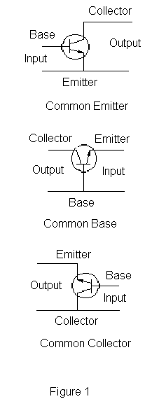
They can be classified in to classes A, B, C & AB. They are defined based on the percent of the cycle of input signal that can produce output current.
4-Bit Analogue to Digital Converter Circuit Diagram
- R1:R2 = 1:2;
- R3:R4:R5 = 1:2:4;
- R6:R7:R8:R9 = 1:2:4:8.

Simple 240VAC TO 5VDC POWER SUPPLY


