Simple Design Subwoofer Box
Labels:
Box,
Design,
Simple,
Subwoofer
0
comments
Boxes are made not based on theoretical , but using the "feeling" that I was the proper size. box if you want a more orderly manner, please use the guide and the calculation of the size of the subwoofer box making a widely circulated on the internet. I took the box with the type of box design for the simple reason ventilated and easy to make. specification of the box that I created can be seen in the picture.
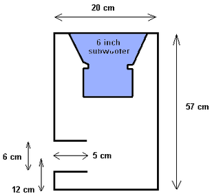
The following are the measures that exist in design subwoofer box :
This box design is not in the specialize for use in cars, such a box is just perfect for a home audio system that is usually used for DVD media player, computer, or game console. subwoofer box actually has a variety of good design for car audio, active speakers, multimedia, and home theater
Basic Theory IC 555
Labels:
555,
Basic,
IC,
Theory
0
comments
Theory Timer 555
Timer 555 is a timer IC that works based on the RC circuit and the comparator is coupled with a digital component (R-Sflip-flop). The first 555 of the type manufactured by Signetics SE-555 working at -55 ° C to 125 ° C and the NE-555 working at 0 ° C-70 ° C. Then 555 is produced with different designs include the LM555, 556 (dual version), and LMC-555 (CMOS version). Timer 555 operates at +5 V dc power supply sd +18 V with temperature stability of 50ppm / ° C (0.005% / ° C). Output 555 can be a current sink / source up to 200mA. IC 555 is compatible with the components of TTL, CMOS op-amps, transistors and other types of linear ICs.
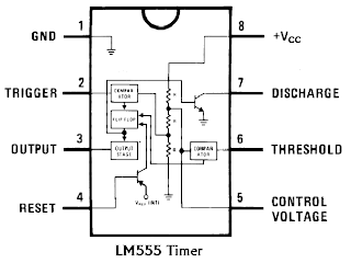
Timer 555 can operate either as a monostable or astable. The resulting square wave output can have a variation of duty cycle ranging from 50 - 99.9% and the frequency of less than 0.1 Hz up to more than 100KHz. 555 Series consists of two voltage comparators (COMP1 and COMP2), a control flip-flop RS (reset / set) that can be reset from outside via the pin 4, an inverting amplifier output (A1), and a discharge transistor (Q1). Kompartor second bias level determined by voltage divider resistors (Ra, Rb, and Rc) contained between Vcc and ground. Inverting input 2/3Vcc komparator1 given input and noninverting input from the given input komparator2 1/3Vcc. Monostable operation requires the input pulse triggers the PIN2 of IC 555. Input trigger voltage drop of more than +2 / 3Vcc toward the voltage is less than + Vcc / 3.
Monostable operation Timer 555
Monostable multivibrator (MMV), also called a one shot, producing a pulse output with a certain period when triggered by a pulse input. Output from Oneshot will instantly go high following the trigger pulse (trigger) and will remain high in accordance with its period. When the period had expired, the output will return low. Outpt Oneshot will remain low until there is another trigger. IC 555 can be operated as MMV by adding an appropriate external circuit.
Both internal comparator prasikap given voltage with a certain voltage level by voltage divider arranged series (Ra, Rb, Rc). Inverting input voltage up to 2/3Vcc komparator1 given, and the noninverting input voltage komparator2 given Vcc / 3. Tersebutlah voltage operation resulted in 555 both as a monostable or astable. External timing circuit (R1C1) connected between Vcc and noninverting input komparator1 through pin6. Pin7 also been linked with causing connected as pin6 transistor to the capacitor C1. When the transistor is on, the resistance of the capacitor is so low that connect (short) through the relationship of CE transistor.
When 555 is connected to the source voltage, input voltage inverting komparator1 will receive registration 2/3Vcc and noninverting input voltage komparator2 would have amounted to Vcc / 3. This causes the RS flip-flop in a reset condition, so that its output Qnot high. Therefore flip-flop connected to the output through an inverting amplifier pin3 (A1) then the output 555 low. In these conditions the capacitor charge (charging). Qnot in the high cause transistor Q1 saturated, which means is connected to ground through a capacitor C1. So in this condition the capacitor to remove the charge (discharge) so that Vc = 0.
If PIN2 give trigger input, when pulsatrigger move towards less than 1/3Vcc voltage as shown in the picture, the noninverting input is more positive than the input komparator2 the inverter , so that the output komparator2 be high. At that time, FIP-flop in the set, so that the output Qnot her low and keuaran 555 high. Because of its low Qnot output, means of transistors in the off. Current flows from Vcc to ground through a capacitor C1. In other words, the capacitor re-charging. (Picture). Capacitor voltage will continue to rise until it reaches 2/3Vcc, at which time the output Vc = 2/3Vcc komparator1 be high and cause the flip-flop is reset and the output 555 back to low. The output 555 will remain until there is another trigger input.
All IC timers rely on an external capacitor to determine the interval of time off-on pulse output. The capacitor would require a certain time to charge or discharge through a resistor. Time can be explained and calculated from the resistance and capacity are given. Equation pulse period to 555 depending on the time required by the capacitor at the time of filling until it reaches 2/3Vcc voltage provided by the RC time constant. Thus, if the capacitor voltage e = E (1 - (-t/RC)), can be calculated time will enable the comparator threshold.
10Hz 60Mhz Frequency Meter
Labels:
10Hz,
60Mhz,
frequency,
Meter
0
comments
The frequency meter can be used to measure the frequency of 10 Hz-60Mhz. The frequency meter has a level of precision or resolution of 10Hz. The frequency meter can be used to measure the frequency of the oscillator, transmitter, frequency generator, cristal, and others during the working frequency trsebut devices in the range 10 Hz - 60MHz. Circuit frequency meter using PIC 16F628A dibagun and with the viewer of the LCD 16 × 2. Frequency meter circuit is working with the working frequency of 4MHz crystal. The series is an electronic frequency meter is quite simple to make. The following picture of the frequency meter circuit.
The series of frequency meters above basically works with the source voltage 5VDC. In this series of 7805 voltage regulator has been installed, so it can be operated with a voltage of 5 - 15VDC.
Microcontroller to RS 485 circuit
Labels:
485,
CIRCUIT,
Microcontroller,
RS,
TO
0
comments
Microcontroller to RS-485 circuit | RS-485 bus can carry up to 256 transceiver modules and over long distances . This is a circuit for connect microcontroller with Rs-485 bus.
Max485Max485 are low-power transceivers for RS-485 and RS-422 communication. Each part contains one driver and one receiver. Line Length vs. Data Rate The RS-485/RS-422 standard covers line lengths up to 4000 feet. For line lengths greater than 4000 feet, see Typical Applications The MAX481, MAX483, MAX485, MAX487–MAX491, and MAX1487 transceivers are designed for bidirectional data communications on multipoint bus transmission lines.
| Microcontroller to RS-485 circuit diagrams |
- In μMAX Package: Smallest 8-Pin SO
- Slew-Rate Limited for Error-Free Data Transmission
- 0.1μA Low-Current Shutdown Mode
- Low Quiescent Current
- -7V to +12V Common-Mode Input Voltage Range
- Three-State Outputs
- 30ns Propagation Delays, 5ns Skew
- Full-Duplex and Half-Duplex Versions Available
- Operate from a Single 5V Supply
- Allows up to 128 Transceivers on the Bus
- Current- Limiting and Thermal Shutdown for Driver Overload
Frequency to Voltage Converter Circuit
IC LM2917 Frequency to Voltage Converter
IC LM2917 IC chip is designed specifically as a Frequency to Voltage Converter or Frequency to Voltage converter. In its use to applications Frequency to Voltage Converter IC LM2917 requires few external components.
There are several examples of applications of Frequency to Voltage Converter IC LM2917 datasheet that is included in the LM2917 IC. In this article series Frequency to Voltage Converter IC also taken from the LM2917 datasheet. The advantages of single chip LM2917 Frequency to Voltage Converter is able to provide instantaneous volt output o at time of frequency change 0 Hz. Very easy to apply in measuring the output frequency with the formulation of single-chip Frequency to Voltage Converter VOUT = FIN x VCC x R1 x C1.
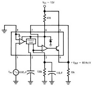
Then the single-chip LM2917 Frequency to Voltage Converter This configuration requires only the RC only in frequency doubling. And has an internal zener regulator to aimlessly accuracy and stability in frequency-to-voltage conversion process.
Application circuit Figure IC LM2917 as Frequency to Voltage Converter
Feature-owned single-chip LM2917 Frequency to Voltage Converter
Reference to ground directly with variable reluctance
Op Amp / Comparator with transistor output
50 mA maximum output currents for application directly to the load
Frequency doubling for low ripel
Buid in zener
Linear output ± 0.3%
Application single chip LM2917 Frequency to Voltage Converter
Frequency to Voltage Converter
Rotation speed sensor applications
Speedometer
Tachometer
Cruise Control
Cluth Control
And other applications associated with the measurement of rotation speed or frequency measurements.
How Regulator with 2 Photocoupler
Labels:
2,
How,
Photocoupler,
REGULATOR,
with
0
comments
Working of Regulator with 2 Photocoupler that is :
- Photocoupler N901 - used as a coupling-off control on the regulator by mikrokontrol. Which is set high and low voltage B + (st-by at the B + voltage is low). Control of the pin-37 POWER mikrokontrol → V610 → VD913 V908 → N901.
- Photocoupler N903 - used to control on-off the regulator of X-ray circuit protector. X-ray protector circuit of flyback → VD451 → VD452 → SCR VS472. If the flyback voltage regulator over the job will automatically be turned off by N903
- To disable the X-ray circuit protector, it can be temporarily removed photocoupler N903 first. In normal conditions the voltage at the transistor V474 should be zero.

| Regulator Schematics |
- Disable by removing the first circuit protectors N903
- Check the voltage of 300V
- Check all transistors
- Check the start voltage of 300V by R909 >> R906 to the base of transistor power regulator
- Check the feedback C910 >> R904 (to oscillate)
Simple Circuit 12V to 120V DC DC Converter
When pin 1 is high transistor Q1 conducts and current flows through the upper half of T1 primary winding. When pin 2 is the transistor Q2 conducts and high current flows through the lower half of the primary coil T1. As a result of a voltage of 120 V AC are induced in the secondary of T1. This voltage is rectified with bridge D1 to provide a 120V DC output. Capacitor C2 is the DC input filter, while C3, C4 are the output filters.
Notes.
- The circuit can be assembled on a vero board.
- Q1 and Q2 require heat sink.
- Output power of this dc dc converter is around 100 watts.
- IC1 and IC2 are to be mounted on holders.
- An optional 5A fuse can be added in series to the 12V supply line.
- T1 can be a 9-0-9V /250V/3A mains transformer.
- If 3A bridge is not available make one using 1N5408 diodes.
- Out of the two Flip-Flops inside CD4013 only one is used here.
- Output of IC1 must be set to 100Hz by adjusting preset R1
Subscribe to:
Posts (Atom)


